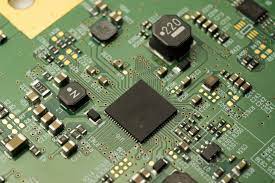
HDI Printed Circuit Board Fabrication
A key component in the success of HDI printed circuit boards is the ability to connect inner layers without passing through the surface layer. This is accomplished through the use of blind vias and buried vias. As component lead pitches continue to shrink, a design team must consider the impact of these finer inner layers and the need to link them with each other as well as to outer surfaces. This is especially true for boards requiring higher levels of functionality or performance in small form factors.
The most common type of PCB via is a through-hole. These holes connect the outer surface of a hdi printed circuit board to its inner layers by drilling a hole through both the copper and the underlying dielectric. These holes are typically larger in diameter than blind or buried vias, which are drilled through just the copper.
During the PCB design process, a designer will determine the location and size of these vias. They are then drilled with precision equipment. The most popular method is to use an excimer laser that can drill through both the copper and underlying dielectric in a single step, avoiding the need for a separate artwork file. These vias require careful calibration to ensure accurate placement and dimensions, allowing a maximum level of connection density.
Blind Vias and Buried Vias in HDI Printed Circuit Board Fabrication
After the blind vias have been drilled, they are filled with an activation solution to promote adhesion between the plated copper and the surrounding dielectric. Then they are capped with an additional copper layer to create the buried vias. The final PCB is then processed through a series of build-up operations to form the inner layers and external connections.
When compared to through-hole vias, blind and buried vias offer the following benefits:
The ability to free up space on the outer surface of the PCB. This allows for a lower layer count and reduced cost, and also helps to improve signal transmission speed and reduce noise.
Buried and blind vias can be combined with microvias to provide access to more layers. This is a great way to improve the functionality of a high-speed signal layer. The additional layer can be used to optimize routing connections and prevent shorting. The additional layer can also be used to lower stub effects and provide an extra buffer against shock and vibration.
In addition to these benefits, buried and blind vias have the advantage of being more reliable than through-hole vias. They are less susceptible to corrosion and can be rerouted easily. The reliability of buried and blind vias depends on several factors, including the quality of the plating, capture pads, and routing connections.
A skilled designer and a good supplier can maximize the benefits of buried and blind vias while keeping costs low. They can use simulation to validate impedance, crosstalk, and other attributes before committing to a stackup. This will allow the designer to optimize their design for a given manufacturing capacity. The resulting board will be compact and highly functional while maintaining excellent quality.